- 您现在的位置:买卖IC网 > Sheet目录3882 > PIC18F4539T-I/ML (Microchip Technology)IC MCU FLASH 12KX16 EE A/D 44QFN
2002 Microchip Technology Inc.
Preliminary
DS30485A-page 181
PIC18FXX39
18.0 COMPATIBLE 10-BIT
ANALOG-TO-DIGITAL
CONVERTER (A/D) MODULE
The Analog-to-Digital (A/D) converter module has five
inputs for the PIC18F2X39 devices and eight for the
PIC18F4X39 devices. This module has the ADCON0
and ADCON1 register definitions that are compatible
with the mid-range A/D module.
The A/D allows conversion of an analog input signal to
a corresponding 10-bit digital number.
The A/D module has four registers:
A/D Result High Register (ADRESH)
A/D Result Low Register (ADRESL)
A/D Control Register 0 (ADCON0)
A/D Control Register 1 (ADCON1)
The ADCON0 register, shown in Register 18-1, con-
trols the operation of the A/D module. The ADCON1
register, shown in Register 18-2, configures the
functions of the port pins.
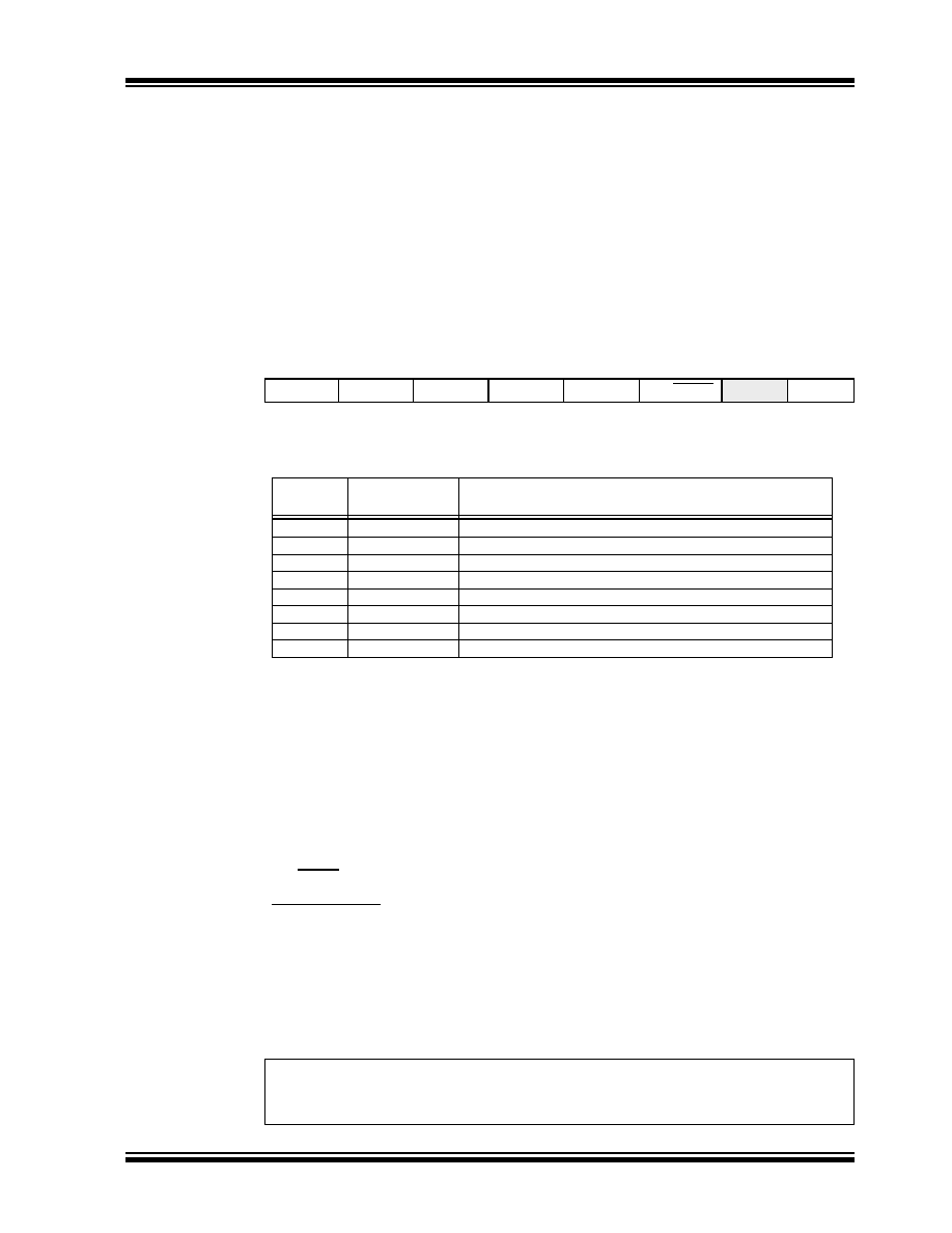
REGISTER 18-1:
ADCON0 REGISTER
R/W-0
U-0
R/W-0
ADCS1
ADCS0
CHS2
CHS1
CHS0
GO/DONE
—ADON
bit 7
bit 0
bit 7-6
ADCS1:ADCS0: A/D Conversion Clock Select bits (ADCON0 bits in bold)
bit 5-3
CHS2:CHS0: Analog Channel Select bits
000
= Channel 0 (AN0)
001
= Channel 1 (AN1)
010
= Channel 2 (AN2)
011
= Channel 3 (AN3)
100
= Channel 4 (AN4)
101
= Channel 5 (AN5)(1)
110
= Channel 6 (AN6)(1)
111
= Channel 7 (AN7)(1)
Note 1: These channels are unimplemented on PIC18F2X39 devices. Do not select any
unimplemented channel.
bit 2
GO/DONE: A/D Conversion Status bit
When ADON = 1:
1
= A/D conversion in progress (setting this bit starts the A/D conversion, which is
automatically cleared by hardware when the A/D conversion is complete)
0
= A/D conversion not in progress
bit 1
Unimplemented: Read as '0'
bit 0
ADON: A/D On bit
1
= A/D converter module is powered up
0
= A/D converter module is shut-off and consumes no operating current
Legend:
R = Readable bit
W = Writable bit
U = Unimplemented bit, read as ‘0’
- n = Value at POR
‘1’ = Bit is set
‘0’ = Bit is cleared
x = Bit is unknown
ADCON1
<ADCS2>
ADCON0
<ADCS1:ADCS0>
Clock Conversion
0
00
FOSC/2
0
01
FOSC/8
0
10
FOSC/32
0
11
FRC (clock derived from the internal A/D RC oscillator)
1
00
FOSC/4
1
01
FOSC/16
1
10
FOSC/64
1
11
FRC (clock derived from the internal A/D RC oscillator)
发布紧急采购,3分钟左右您将得到回复。
相关PDF资料
PIC18LF2539T-I/SO
IC MCU FLASH 12KX16 EE AD 28SOIC
PIC18LF4539T-I/PT
IC MCU FLASH 12KX16 EE AD 44TQFP
PIC16LF874AT-I/ML
IC MCU FLASH 4KX14 A/D 44QFN
PIC16F77T-E/ML
IC MCU FLASH 8KX14 A/D 44QFN
PIC16F874A-E/ML
IC MCU FLASH 4KX14 A/D 44QFN
PIC16F74T-I/ML
IC MCU FLASH 4KX14 A/D 44QFN
PIC16F77T-I/ML
IC MCU FLASH 8KX14 A/D 44QFN
PIC18F24K20-I/SS
IC PIC MCU FLASH 8KX16 28SSOP
相关代理商/技术参数
PIC18F4539T-I/PT
功能描述:8位微控制器 -MCU 24KB 1408 RAM 32 I/O RoHS:否 制造商:Silicon Labs 核心:8051 处理器系列:C8051F39x 数据总线宽度:8 bit 最大时钟频率:50 MHz 程序存储器大小:16 KB 数据 RAM 大小:1 KB 片上 ADC:Yes 工作电源电压:1.8 V to 3.6 V 工作温度范围:- 40 C to + 105 C 封装 / 箱体:QFN-20 安装风格:SMD/SMT
PIC18F4550EPT
制造商:Microchip Technology Inc 功能描述:
PIC18F4550-I/ML
功能描述:8位微控制器 -MCU 32kBF 2048RM FSUSB2 RoHS:否 制造商:Silicon Labs 核心:8051 处理器系列:C8051F39x 数据总线宽度:8 bit 最大时钟频率:50 MHz 程序存储器大小:16 KB 数据 RAM 大小:1 KB 片上 ADC:Yes 工作电源电压:1.8 V to 3.6 V 工作温度范围:- 40 C to + 105 C 封装 / 箱体:QFN-20 安装风格:SMD/SMT
PIC18F4550-I/P
功能描述:8位微控制器 -MCU 32kBF 2048RM FSUSB2 RoHS:否 制造商:Silicon Labs 核心:8051 处理器系列:C8051F39x 数据总线宽度:8 bit 最大时钟频率:50 MHz 程序存储器大小:16 KB 数据 RAM 大小:1 KB 片上 ADC:Yes 工作电源电压:1.8 V to 3.6 V 工作温度范围:- 40 C to + 105 C 封装 / 箱体:QFN-20 安装风格:SMD/SMT
PIC18F4550-I/PT
功能描述:8位微控制器 -MCU 32kBF 2048RM FSUSB2 RoHS:否 制造商:Silicon Labs 核心:8051 处理器系列:C8051F39x 数据总线宽度:8 bit 最大时钟频率:50 MHz 程序存储器大小:16 KB 数据 RAM 大小:1 KB 片上 ADC:Yes 工作电源电压:1.8 V to 3.6 V 工作温度范围:- 40 C to + 105 C 封装 / 箱体:QFN-20 安装风格:SMD/SMT
PIC18F4550T-I/ML
功能描述:8位微控制器 -MCU 32kBF 2048RM FSUSB2 RoHS:否 制造商:Silicon Labs 核心:8051 处理器系列:C8051F39x 数据总线宽度:8 bit 最大时钟频率:50 MHz 程序存储器大小:16 KB 数据 RAM 大小:1 KB 片上 ADC:Yes 工作电源电压:1.8 V to 3.6 V 工作温度范围:- 40 C to + 105 C 封装 / 箱体:QFN-20 安装风格:SMD/SMT
PIC18F4550T-I/PT
功能描述:8位微控制器 -MCU 32kBF 2048RM FSUSB2 RoHS:否 制造商:Silicon Labs 核心:8051 处理器系列:C8051F39x 数据总线宽度:8 bit 最大时钟频率:50 MHz 程序存储器大小:16 KB 数据 RAM 大小:1 KB 片上 ADC:Yes 工作电源电压:1.8 V to 3.6 V 工作温度范围:- 40 C to + 105 C 封装 / 箱体:QFN-20 安装风格:SMD/SMT
PIC18F4553-I/ML
功能描述:8位微控制器 -MCU 32KB FLSH 2048 RAM FSUSB 2.0 12B ADC RoHS:否 制造商:Silicon Labs 核心:8051 处理器系列:C8051F39x 数据总线宽度:8 bit 最大时钟频率:50 MHz 程序存储器大小:16 KB 数据 RAM 大小:1 KB 片上 ADC:Yes 工作电源电压:1.8 V to 3.6 V 工作温度范围:- 40 C to + 105 C 封装 / 箱体:QFN-20 安装风格:SMD/SMT